Introduction
This article covers everything you need to know about lab benches and their applications.
You will learn about:
- What a Lab Bench is
- Different Types of Lab Benches
- How Lab Benches are Manufactured
- Common Uses of Lab Benches
- And much more...
Chapter 1: What is a Lab Bench?
A laboratory bench is a specialized table designed to facilitate various lab tasks and experiments, including handling reagents and test specimens. During manufacturing, these benches incorporate corrosion-resistant finishes and vibration-reducing features to maintain test accuracy and experimental precision.
As the central component of most research labs, lab benches are typically the largest and most essential furniture in scientific, R&D, and experimental settings. They provide sturdy, smooth, and non-porous work surfaces with integrated connections and accessories to support critical laboratory activities.

The term "lab bench" refers to workstations engineered to meet specific requirements of various laboratory environments. Selection depends primarily on the intended use, with the main distinction being between wet and dry lab benches. Dry lab benches typically feature large work surfaces, electrical connections, and ample storage, while wet lab benches are designed for liquid handling with features like vessel storage racks, sinks, and more compact work areas.
Chapter 2: What are the Different Types of Lab Benches?
Every piece of laboratory furniture is carefully selected to meet specific operational needs. The lab design process begins with choosing the appropriate lab bench, which is determined by the nature of the scientific work. A key consideration is the work surface, designed for either wet or dry laboratory processes based on chemical or biological research requirements.
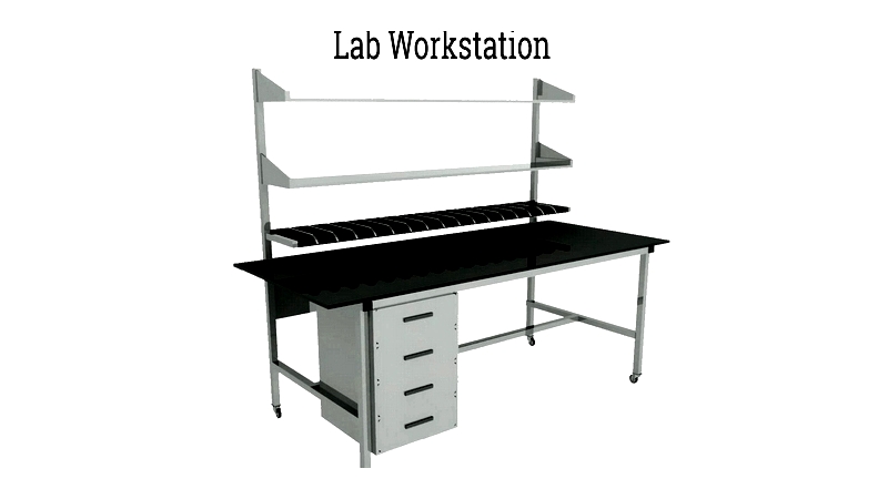
Lab benches serve as the foundation for laboratory operations, providing durable workspaces for experiments and sample preparation. While they may appear simple, modern laboratory benches incorporate integrated storage, utilities, and specialized accessories to support diverse tasks that would be impractical on standard workbenches.
Lab Bench Classification
Lab benches can be categorized by function, structure, and purpose. Each classification includes subcategories detailing specific configurations to ensure safety, efficiency, and compliance with laboratory standards.
Classification by Function
Functional classifications are based on supported lab activities:
- Physical Lab Benches: Designed for electronics, electrical testing, and other dry processes, often featuring anti-static surfaces or vibration isolation.
- Chemical Lab Benches: Suitable for chemical studies and reactions, available in wet or dry configurations with resistant surfaces.
- Biological Lab Benches: Equipped for microbiology and genetic research, often including sinks, containment features, and incubation equipment.
Classification by Structure
Structural classifications include:
- Floor-Mounted Lab Benches: Heavy-duty bases with durable surfaces, ideal for general or equipment-heavy labs.
- Suspended Lab Benches: Wall-mounted for easy cleaning and utility access, featuring modular components.
- Mobile Lab Benches: Wheeled for flexibility, incorporating robust frames and storage features.
Classification by Purpose
Purpose-based categories include:
- Island Benches: Central workstations for collaborative research.
- Side Benches: Wall-mounted for individual workspaces.
- Sink Benches: Equipped with plumbing for liquid handling.
- Reagent Racks: Specialized storage for chemicals and consumables.
Traditional Lab Benches
Traditional lab benches offer versatile, cost-effective solutions for general laboratory use. They feature sturdy construction and adaptable designs suitable for academic and training environments.
Custom Laboratory Workbenches
Custom lab workbenches address specialized research needs with tailored designs. These benches incorporate unique features like adjustable heights, integrated utilities, and specialized materials to support advanced scientific work.
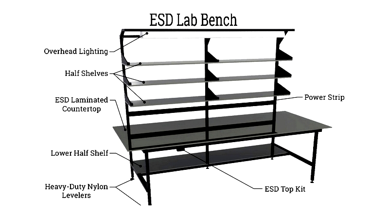
Electrostatic Dissipative (ESD) Bench
ESD lab benches prevent static discharge in electronics labs, featuring grounded surfaces to protect sensitive components.
Mobile Lab Benches
Mobile benches provide flexible workspace solutions, easily repositioned to accommodate changing lab requirements.

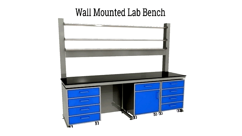
Wall Mounted Lab Benches
Wall-mounted benches optimize space in compact labs, often incorporating plumbing and electrical connections.
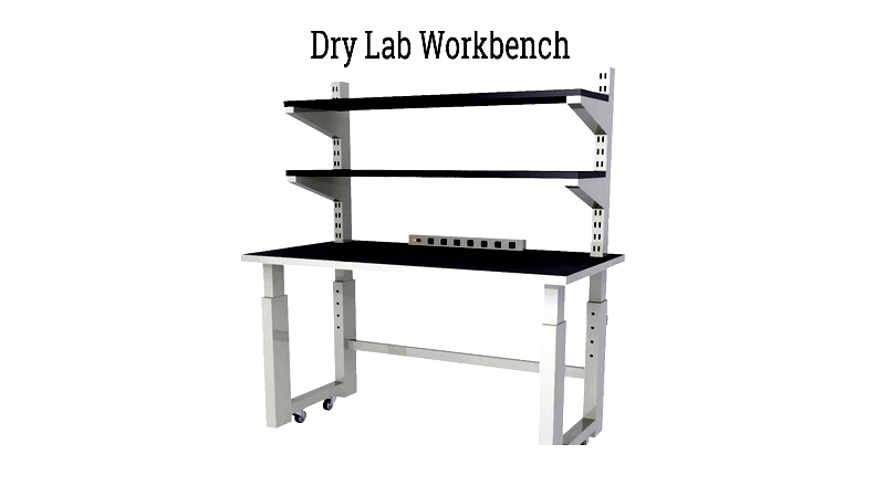
Dry Lab Benches
Designed for computational and analytical work, dry lab benches feature stable surfaces with integrated power management.
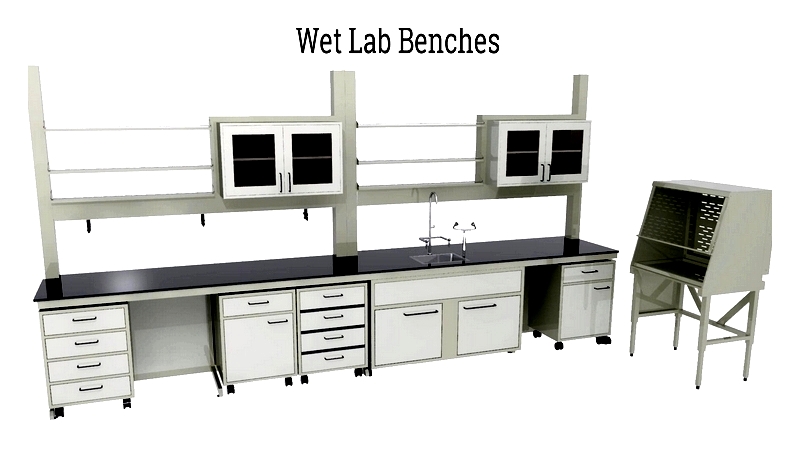
Wet Lab Benches
Wet lab benches support liquid handling with chemical-resistant surfaces and integrated waste management features.
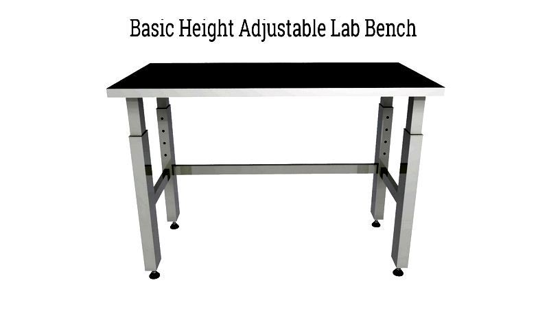
Ergonomic Lab Benches
Ergonomic benches promote worker comfort and safety with adjustable features designed for prolonged laboratory work.

Laboratory Tables
Versatile laboratory tables provide adaptable work surfaces for various research and production applications.
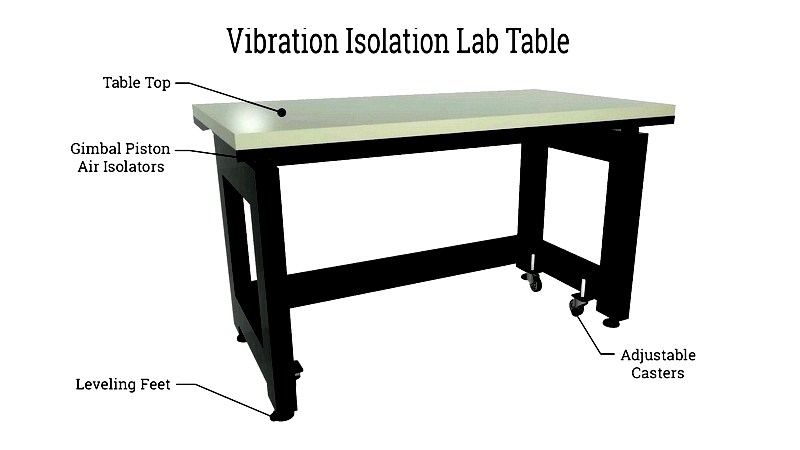
Vibration Isolation Lab Tables
These specialized tables minimize vibrations for precision instruments, ensuring accurate measurements in sensitive environments.